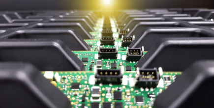
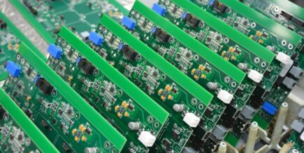
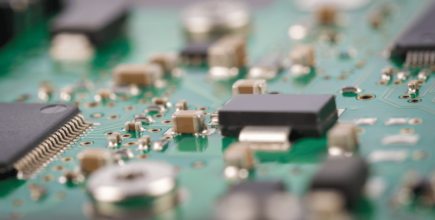
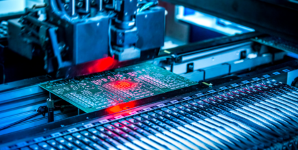
Skip to Content
Exit

Tag Archive: pcb assembly

  1. 6 Common Design Concerns with PCBAs

    Leave a Comment

    Before PGF, There’s the Design

    Designing a Printed Circuit Board Assembly (PCBA) can be a complex task, and engineers must take into account many concerns to ensure that the assembly functions correctly and meets all the requirements. These concerns include everything from the layout and routing of the circuits to the selection of components and materials. Before starting with the PGF partnership, a company must first solidify its design for the assembly process. 


    1. Proper Routing

    One of the most important design concerns in PCB Assembly is ensuring the proper routing of the circuits. This means that the pathways for electrical current are clear and free of any obstacles that could cause a short circuit or other problems. The routing of the circuits must also take into account the power requirements of the components, as well as any potential electromagnetic interference (EMI) that could affect the functioning of the assembly.


    2. Layout of Components

    Another important design concern is the layout of the components on the PCBA. Engineers must carefully consider the placement of the components to ensure easy assembly and enough space for them to function properly. The layout must also take into account the thermal characteristics of the components, as some components may generate more heat than others, and the layout should dissipate this heat effectively.


    3. Component Selection

    Component selection is also an important design concern. Chosen components must be appropriate for the application and compatible with the PCBA. This designation includes not only electronic components but also the materials used on PCBAs such as the substrate, copper thickness, solder mask, etc. Engineers should select them based on their specifications and characteristics, such as power dissipation and operating temperature range, and should be of good quality to ensure that they function correctly and have a long service life.


    4. Safety and Compliance Requirements

    The PCB Assembly must meet any necessary safety and compliance requirements. PCBAs in medical devices, for example, must meet stringent safety and performance standards set by certifications such as ISO 13485:2016. This includes ensuring that the materials and components in the assembly are safe for use in a medical environment and that the assembly is properly shielded to protect against electromagnetic interference. Similarly, PCBAs used in other applications such as industrial or aerospace must meet relevant compliance and safety standards.


    5. Testing and Validation

    Another important design concern is testing and validation of the PCB Assembly. The functionality of the PCB Assembly must be verified through various testing methods such as visual inspection, continuity testing, in-circuit testing, and functional testing to ensure that it meets the specifications and requirements of the application. Some machines to assist with the testing process include X-ray and AOI Inspection. This testing must happen at different stages of the assembly process to ensure the early detection and correction of any problems.


    6. Cost

    Finally, the cost is always a concern when designing a PCB Assembly. PCBAs can be expensive to manufacture, and the cost of components and materials can add up quickly. To minimize costs, the designer must consider the most cost-effective components and materials and use them in the assembly. Additionally, the design should be optimized to minimize the number of components and the size of the PCBA, while still meeting all the requirements.


    Summary

    In conclusion, designing a Printed Circuit Board Assembly involves many design concerns that need to be taken into account. Proper routing and layout of circuits, component selection, safety and compliance, testing and validation, and cost are key design concerns that engineers need to address to ensure that the PCB assembly functions correctly and meets all requirements. Skilled engineers and designers with experience in PCBA design and assembly can help to confirm functionality and feasibility before starting with your contract manufacturer. At PGF, you design it, and we’ll build it! 

    LinkedIn LogoYouTube LogoTwitter LogoFacebook Logo

  2. Box Build Assembly

    Leave a Comment

    What is a Box Build Assembly?

    A box build assembly incorporates the manufacturing of both cables and printed circuit boards. Box builds consist of a single enclosure holding various complex electromechanical components. The combination of PCB and cable manufacturing involves a process involving intricate design, production, and construction for each unit. Additionally, box builds include an immense opportunity for customization in size, wiring specifications, and enclosure fabrication. PGF Technology Group offers a wide selection of enclosure types ranging from weatherproof to plastic materials. PGF dedicates itself to ensuring high-quality services and proper assemblies for each project and partner!

    Box Build Applications

    Box build assemblies are utilized in a variety of different industries and for a multitude of purposes. In practice, box builds have many integral applications in the advancing world of technology and electronics. Whether the box build is large or small, its importance to growing fields and daily conveniences continues to increase exponentially. From computers to industrial machines, each application demonstrates an industry seeking the capabilities of box-build assemblies for critical purposes. 

    Box Build Assembly Infographic

    Computer

    The growing dependency on computers increases the demand for box builds. Complex software requires immense wiring connections and electrical systems for the highest performance quality.

    Aerospace and Defense

    The highly critical aerospace field requires error-free and trustworthy devices such as design-specific box builds. To ensure the utmost safety, the aerospace industry requires proper box build enclosures and reliable electronic processes. 

    Industrial Machinery

    The necessity for high productivity and performance distinguishes the need for box build industrial electronic devices. For protection purposes, the addition of PCBAs and wiring guarantees smooth operation in environmentally stressful conditions. 

    Data Cable

    A data cable box build is a common assembly that greatly varies from project to project. With the immense selection in size, such assemblies are customized based on their intended location. Typically, larger data cable assemblies are found in sizeable buildings. For example, skyscrapers, hotels, and even substantial homes generally hold data cable box builds.

    Environmental Protection 

    The box build structure differs from traditional assemblies in that the cables and printed circuit boards are protected through a physical barrier. Additionally, the entirety of the box build can be found within the external box aiding in the assembly process. Yet, in some instances, the barrier safely protects its components from extreme weather conditions, abrasion, physical destruction, and oil.

    PGF Excellence

    PGF’s cross-trained and qualified personnel provide efficient and high-quality box build assemblies. A PGF partnership benefits customers in the vast opportunity for customization as well as simplifying the supply chain assembly. With professional knowledge in box build assembly, PGF can lower production costs by accessing lower-priced components. Additionally, with both cable and PCB expertise PGF can provide box build services under a single warehouse, decreasing overhead costs. As for a simplified supply chain, PGF assembles box builds entirely in-house, thus removing potential conflict points for customers. PGF is a solutions provider relieving customers of the unnecessary stress of logistics and manufacturing. Request a quote today and learn more about the ways PGF can assist in all box build assembly needs!

    LinkedIn LogoYouTube LogoTwitter LogoFacebook Logo

  3. PCB Mounting Techniques

    Leave a Comment

    What is a PCB?

    Printed Circuit Boards, or PCBs, hold a variety of functions, sizes, and industrial applications. To add electrical components to the board, PCB assemblers utilize either surface or through-hole mounting methods. PGF Technology Group prides itself on offering both PCB techniques, with optional combinations of  SMT or through-hole technologies. By staying on the edge of technology, PGF continues to further integrate surface-mounting techniques to all applicable assemblies, saving both time and money. However, although the surface mounting techniques take precedent, PGF continues to provide authentic through-hole processes to best suit customer specifications. The presence of both techniques widens the PGF market, thus utilizing either process based on the most efficient solution.

    Surface Mounting

    The surface mounting PCB assembly method involves mounting electrical components onto the top of the printed circuit board. With surface mount technology (SMT), electrical components are installed in a simple and timely manner. The surface-mounting technique allows ample use of both sides of the board. Surface mounting SMT technologies automate the assembly process, increasing production speed while maintaining high-quality products. The Fuji and MyData machines are the two main types of machinery used to process PCBs.

    PCB Techniques Infographic

    Benefits:

    • Allows for smaller PCB design, closely placed components
    • Compact and lightweight
    • Cost-effective with faster production time
    • More efficient designs with components aligned tighter together
    • More controlled manufacturing environment from automated machine technology


    Through-Hole Mounting 

    Through-hole mounting involves a pre-drilled hole to install and solder the electrical component to the printed circuit board. Typically used for large components, the through-hole method may also be utilized for attaching components determined incompatible with the surface mount technologies. Before SMT advanced automating technologies, the through-hole method was the main assembly practice to attach components to the board. While through-hole mounting is not as common, particularly military and aerospace industries utilize such methods to ensure durability in irregular conditions.


    Benefits:

    • With components attached through the board, such PCBs offer higher strength and reliability
    • Able to endure larger amounts of external physical stressors
    • Easily replaceable and thus desirable for various testing endeavors or prototyping projects
    • Ability to withstand higher heat capacities
    • The stronger bond between the board and the electrical components allows higher power capabilities


    PGF Premium Services

    While offering both surface mounting and through-hole mounting techniques, PGF delivers high-quality products that meet all customer specifications promptly. Additionally, PGF offers X-Ray Evaluations and Ionograph Testing services to all customers, showcasing the company’s dedication to excellence. Learn more about the endless PGF advantages for all your PCB needs. Request a quote and experience all PGF premium services today!

    LinkedIn LogoYouTube LogoTwitter LogoFacebook Logo

  4. A Complete Prototyping Checklist for Printed Circuit Boards (PCBs)

    Leave a Comment

    The pillars of quality electronic manufacturing are precision, reliability, and functionality. Each project must meet a specific performance standard, and printed circuit boards (PCBs) are critical in gauging whether a project has succeeded or failed. PCB assembly systems risk becoming unreliable, imprecise, and nonfunctional without proper manufacturing. Prototyping is an essential step to guarantee these products function as planned. In effect, this blog breaks down the prototyping checklist and the benefits of the process. 

    Benefits of Prototypes

    benefits of pcba prototypingPrototypes for PCBs help prevent potential issues with the end product. Prototyping offers numerous advantages, such as:

    Trained Eye Inspection

    Firstly, multiple tests at every step ensure the project meets the original vision. In practice, tests involve a trained eye inspection of the product’s design, followed by specific testing methods, including automated optical inspection (AOI), solder paste inspection (SPI), and X-ray evaluations.

    Supreme Time-Saver and Performance-Checker

    Testing individual components enable manufacturers to pinpoint areas of failure in designs accurately. This process is critical, as a single defective piece is detrimental to a project. Simultaneously testing each feature helps optimize performance and save time.

    Open-Line Discussion with Manufacturer

    Prototype assemblies entail open communication with manufacturers. If certain areas require more focus than others, it’s easy to connect with the manufacturer to relay this need. Manufacturers will break down references, product life, component cost allocation, and documentation. Additionally, they can troubleshoot any problems that develop.

    Early Discovery of Design Problems

    Prototypes help ease the consequences of errors by providing sufficient time to fix design flaws or readjust concepts. This benefit stops issues from becoming more critical as manufacturers produce higher volumes, preventing resource waste and project delays.

    Reduce Added Costs

    Another benefit of prototyping is the ability to discover pitfalls on the road map instead of detecting fatal flaws at a later time. This step saves more money by ensuring successful production and replication.

    Shorten Project Timeline

    Prototyping helps avoid the winding roadblock and U-turns that could otherwise lengthen a project’s timeline. When developing new product designs, their impact on a given industry depends on their timing and effectiveness. 

    Prototyping Checklist for Success

    To help you get started on your next project, here’s a prototyping checklist that will guide you through each step to ensure your project’s success. These steps are as follows:

    1. 1. Send initial documents and design specifications
    2. 2. Receive feedback from PCBA manufacturers on the company and  initial machine compatibility
    3. 3. Receive a review of the bill of materials with a focus on end-of-life components
    4. 4. Review the visual model of the design with the manufacturer to ensure the project is feasible
    5. 5. Make any necessary adjustments to the PCBA design
    6. 6. Review the proof-of-concept (POC) with the manufacturer for a final check of feasibility
    7. 7. Make additional adjustments to the PCBA design as needed
    8. 8. Review the performance of the working prototype with the manufacturer to check functionality
    9. 9. Make more adjustments to the PCBA design if required
    10. 10. Review the functional prototype with the manufacturer for a final check of functionality
    11. 11. Make final necessary adjustments to the PCBA design
    12. 12. Greenlight the project for production

    pcb assembly guide to prototyping

    PCB Assembly and Prototyping at PGF Technology Group, Inc.

    If you require reliable PCB assembly and prototyping for a project, PGF Technology Group offers complete PCB assembly services to help fully realize your vision. We have worked with many customers across many industries, including:

    We’ll work with you to determine what you need for your unique project based on your specifications. We’ll then prototype the end product to ensure it’s fully functional and features an accurate and precise design. Contact us today to get started on your next project with us or learn more about our services

    Contact Us

  5. Design for a Medical PCB Assembly

    Leave a Comment

    Playing the Game

    When it comes to medical devices, no average or sub-par printed circuit board assembly (PCBA) is going to cut it! In this live-action game of Operation, the consequences are real, and the assembly is accountable.

    As a premier manufacturer of printed circuit boards, PGF Technology Group fully understands the importance of proper PCBA design for medical devices and systems. However, some may find the design process challenging since many factors must be considered. These factors include safety requirements, cleanliness standards, industry/application-specific regulations, and more. That’s why our team has put together the following guide, which goes over some of the key considerations to keep in mind when designing medical PCB assemblies.


    Design for Medical PCBA InfographicSafety First

    Accuracy and precision are crucial to avoiding the buzzer. Many medical devices are designed to perform vital functions while living in or on the human body for extended periods, such as insulin pumps and pacemakers so that any malfunction can put the patient’s life at risk. That’s why manufacturers must design and build these products and their components carefully to ensure patient safety. PCBA manufacturers should consider the operational and environmental conditions (e.g., fluid exposure, temperature), their effect on the product, and the measures needed to combat those effects.


    Cleanliness Is Close to Godliness

    A clean workplace is a safe workplace. This saying is especially pertinent in the medical industry, where cleanliness can significantly affect the health and wellbeing of patients and the performance and lifespan of devices. That’s why PCBA manufacturers will often use materials that form surfaces that are easy to clean and disinfect and incorporate strict cleaning practices into production operations to remove any residues left behind from manufacturing processes. Additionally, according to the cleanliness of product clause in ISO 13485 Medical Devices — Quality Management Systems — Requirements for regulatory purposes, organizations need to document product cleanliness or contamination control requirements.


    Read the Rule Book

    To properly play the game, you have to know the rules. In the medical industry, products are subject to numerous regulations outlining how they should be designed, manufactured, used, etc. Knowing, understanding, and following them is essential to the success of a product.


    ISO 13485

    Firstly, one of the most critical regulations relevant to medical PCBAs and other electronics is ISO 13485, which establishes the requirements for quality management systems for companies involved in one or more of the lifecycle stages of a medical device or the supply of products. The 2016 update of the standard brought the requirements in line with those already mandated by the FDA.

    Companies can be certified to this standard, meaning their quality management system has been verified to meet its strict requirements. The requirements aim to ensure the production of high-quality medical products that are safe and effective, which is why many countries require medical device companies to attain certification. In addition, ISO 13485 certified companies benefit from higher customer satisfaction, greater customer trust, and better credibility.


    IPC Class 3 Standards

    Other specifications to consider are the IPC Class 3 Standards. Companies that meet these specifications value skill, constant improvement, and intense scrutiny. They know that a buzzer in the game signals a life or death scenario, so practices must be monitored and perfected.


    PGF Technology Group maintains the ISO 13485 compliance and IPC Class 3 Standards for any project connected to medical devices.


    What’s the Use?

    In addition to safety, manufacturers must keep in mind the usability of PCBAs. For example:

    • Is SMT or thru-hole assembly appropriate? Manufacturers should reference the specific design requirements from the client to ensure that they utilize the best method of assembly. This process may include prototypes to review board real estate and functionality.
    • How small is too small? While it can be tempting to go with the smallest PCBA design, a design that is too small can limit the complexity of your device. You need to ensure enough space to incorporate all components for a fully operational and reliable instrument.
    • What is the min/max amount of energy input? Determine the circuit’s energy to run during typical and peak operation.


    Making It Easy

    Anyone who has built an IKEA item understands the pain caused by a hard-to-assemble project. Without clear-cut instructions and imagery to demonstrate design, the process can become prolonged. Medical PCBA designers can eliminate this pain by designing with assembly in mind; assemblers should not have trouble reaching and mating cables to connectors, soldering connections or placing other essential components. Additionally, the assembled product should be testable using various methods. Some examples include visual assessment, Solder Paste Inspection (SPI), X-ray scanning, In-Circuit Testing (ICT), and Automated Optical Inspection (AOI).


    Medical Device Solutions at PGF Technology

    Want to learn more about the critical design considerations for medical PCB assembly? Ask the experts at PGF Technology Group! As an ISO 13485 certified company specializing in PCBA, we can answer or address any of your questions and concerns. Importantly, you can check out our eBook, Key Considerations for Medical PCB Assembly, to overview the vital considerations to keep in mind when designing and assembling medical PCBAs.

    At PGF Technology, we have the knowledge, experience, and certifications to deliver PCBA solutions that meet the most stringent specifications. Contact us or request a quote today if you want to partner with us for your medical PCBA needs.

    LinkedIn LogoYouTube LogoTwitter LogoFacebook Logo

Have Any Questions?

Click Here Now > X