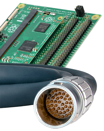

Printed circuit board assemblies (PCBAs) are used in a variety of industrial and consumer electronics, ranging from military weaponry to remote controls. PCB Assemblies can be adapted to suit circuits of any complexity.
Though PCBAs are relatively commonplace, their complexity makes it critical to source new circuit board assemblies from reliable suppliers. PGF Technology Group provides comprehensive printed circuit board assembly manufacturing services, building to spec for diverse industries, from aerospace to medical to industrial equipment and more.
Surface-mount technology (SMT) involves direct mounting of components on top of of the PCB using solder paste. SMT PCB assembly is the current industry standard for almost all consumer electronics due to the demand for miniaturization and high power density. Offering high component density, automated production, and a lower cost for mass production, SMT has revolutionized electronics by allowing for smaller, lighter, and faster assemblies.

In through-hole technology (THT), components are inserted into pre-drilled holes on the PCB and soldered into place on the opposite side. It remains the classic PCB assembly method for certain applications. Ideal for industrial control switches and high-voltage power supplies, THT offers exceptional mechanical bond strength, ease of repair, and high-heat tolerance.
While SMT and THT have their own sets of ideal applications, sometimes mixed technology assembly is the best option. In this hybrid approach, both through-hole and surface-mount components are assembled onto the same PCBA. Mixed technology assembly is common in products that require both high-power handling and compact electronics.
Our PCBA manufacturing services involve putting together the substrate and electronic components.
This base material is typically made of fiberglass-reinforced epoxy resin (FR-4), with various layers on top:
A solder mask is a protective layer of material applied over the circuit board, serving to insulate and shield conductive traces and prevent solder bridges during the soldering process. The solder mask is responsible for a PCB’s characteristic green color.
The silkscreen is a screen-printed layer that provides assembly and reference information for the PCB. The silkscreen is usually white text on the green solder mask.
Copper layers refer to thin sheets of copper that are laminated onto the surface of the circuit board, forming conductive pathways for electrical signals and power distribution. Every PCB contains one or more copper layers, including the etched pathways (traces) that form the circuit.
Based on the needs of your application, these may include capacitors, resistors, and integrated circuits (ICs) soldered onto the substrate. Together, the components create a functional electronic module.
PGF Technology offers the following PCB assembly types:

The most straightforward and most affordable PCBs consist of one copper layer laminated to a non-conductive substrate layer. One side of the board contains all pathways.

A more versatile option, double-sided PCBs incorporate circuitry on both sides of the PCB. These boards have three total layers, consisting of two layers of copper on either side of a non-conductive substrate.
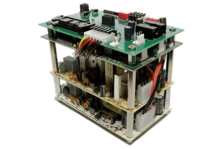
The most complex and expensive, multi-layer PCBs enable intricate circuitry that would be impossible to contain in one or two layers. These boards allow for maximum component density by moving some traces to the board’s interior, freeing room for additional SMT components on the exterior.
Using state-of-the-art machinery, PGF Technology Group can handle surface mount, through-hole, and mixed-technology assembly. We also offer integrated electromechanical assembly services for customers seeking larger sub-assemblies or complete products. Electromechanical assembly, also called box build assembly, combines a completed PCBA with corresponding electronic components and harnesses to yield a functional product.
When you choose PGF Technology, you’ll benefit from our end-to-end PCB assembly capabilities, which improve the overall quality of the PCBAs, shorten time to market, and reduce production costs.
Our advanced PCB assembly capabilities always adhere to the highest industry standards. Between receiving, assembly, testing, and shipping, our facility manages your project with attention and dedication.
Explore our PCB assembly methods below:


Automated assembly is ideal for components that are difficult to solder by hand and high-volume production runs. It is the fastest and most efficient means of producing consistent circuit boards.

Reflow soldering is the most common method used for efficiently soldering SMT-mounted components. The process uses a reflow oven to melt solder onto a pre-heated and pre-soaked PCB.

Wave soldering is another efficient method that involves applying flux to an entire PCB surface, heating the board, and then applying molten solder to the whole heated board. This process has been greatly dismissed due to the addition of selective soldering.

Selective solder is a more precise variation of wave soldering used to apply flux locally rather than the entire PCB. Instead of using a “wave” of molten solder, it uses nozzles to apply solder exactly where needed.

Hand insertion and soldering may be used when project constraints require manual through-mounting.

In-circuit testing (ICT) involves the use of a specialized test fixture that contains probes or pins. ICT verifies the integrity of individual components, checks for proper circuit connectivity, and detects potential defects such as short circuits, open circuits, or incorrect component values.

This automated inspection process uses cameras to scan the PCB for defects and quality issues.

The SPI process closely inspects solder paste deposition before part placement.
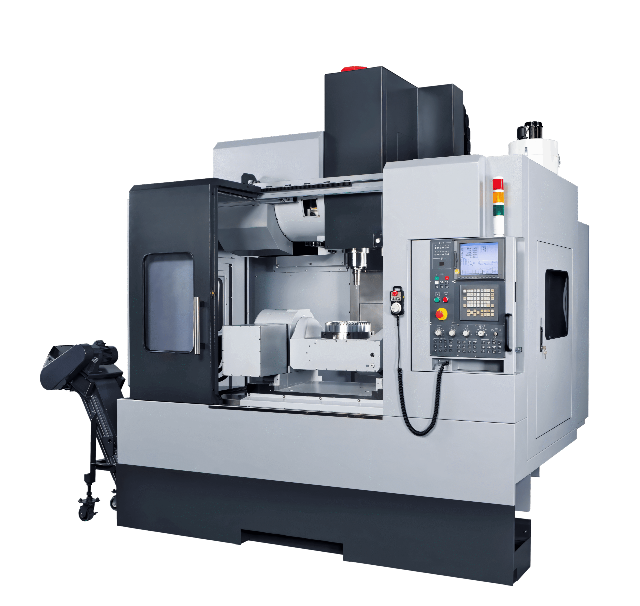
PCBAs find extensive applications in products such as smartphones, automotive control systems, communication devices, medical monitors, manufacturing machinery, and satellite systems, enabling efficient electronic functionality in diverse sectors.




At PGF Technology, our skilled and knowledgeable team conducts routine inspections and continuity testing to identify the following types of potential defects in manufactured components:
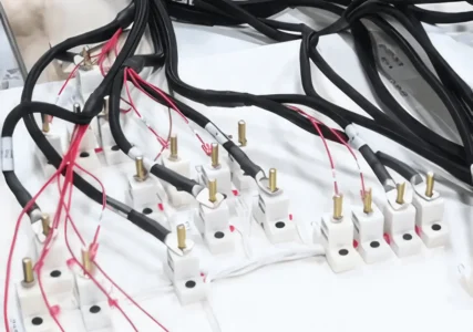
With advanced testing equipment, we can verify the integrity of wire connections in our custom cable assemblies, ensuring optimal performance and reliability.
WIRE HARNESS / CABLE PROCESS
Each wire termination is subjected to a calibrated tensile force to verify the mechanical integrity of every crimp joint before the assembly ships.
Using our Cirris tester, every conductor path is electrically verified — ensuring no open circuits, shorts, or miswired connections reach your product.
Inspectors review each completed harness for routing accuracy, connector seating, insulation condition, and proper labeling across the full assembly.
PCBA PROCESS
High-resolution cameras automatically scan every completed board, detecting solder bridges, missing components, and misalignments without manual intervention.
Trained technicians manually review each board for workmanship quality, component orientation, and assembly details that automated systems may not catch.
One transposed connection can make an entire assembly non-functional — or damage downstream equipment. Continuity testing catches miswiring at the source.
Every electrical pathway is verified to confirm complete circuit continuity and proper signal flow across all connections on the finished board.
All of our Made-in-the-USA complex cable assemblies adhere to strict regulatory standards. The following certifications represent our commitment to providing the highest level of safety, quality, and reliability:
After conducting a final functional and visual inspection, we deliver products for seamless installation into the intended devices or systems.



Precision PCB Assembly From PGF Tech
PGF Technology Group provides state-of-the-art PCB assembly for surface mount, through-hole, and mixed-technology applications. Since 1970, we have provided reliable contract assembly manufacturing for customers in critical industries. We specialize in high-mix, low-volume build-to-spec PCBAs, box builds, and wire harness and cable assemblies, with a history of partnering with our clients to deliver high-quality solutions.
Request a quote to start your custom PCB assembly manufacturing project.
PGF Technology Group utilizes state-of-the-art automated assembly lines to support a full range of technologies, including Surface Mount Technology (SMT), Through-Hole (THT), and mixed-technology assemblies. Our high-speed placement equipment is capable of handling the latest component packages, from 01005 miniatures to large fine-pitch BGAs (Ball Grid Arrays). We also specialize in double-sided SMT and complex multi-layer boards.
Yes, we offer flexible engagement models to suit your procurement strategy. Under our Full Turnkey service, we manage the entire process—including component sourcing, PCB fabrication, assembly, and testing. Alternatively, we offer Consigned services where you provide the components and boards, and we handle the precision assembly. Many clients also choose a Partial Turnkey hybrid model to maintain control over specific long-lead items while leveraging our supply chain for standard components.
Quality is at the core of everything we build. We are ISO 9001:2015 certified and our technicians are trained to IPC-A-620 standards, the industry benchmark for cable and wire harness fabrication. We perform 100% electrical testing on every assembly to ensure continuity and proper pin-out configuration. Additionally, we conduct pull-force testing and visual inspections throughout the manufacturing process to guarantee long-term reliability in the field.
Absolutely. We understand that getting a functional prototype quickly is vital for design validation. PGF has a dedicated workflow for rapid prototyping and low-volume production runs, allowing you to move from CAD files to physical boards in days rather than weeks. Our engineering team also provides “Design for Manufacturability” (DFM) feedback during this phase to help streamline your transition into high-volume production.
We offer a comprehensive suite of testing options to ensure your boards perform flawlessly in the field. Beyond visual and X-ray inspection, we provide In-Circuit Testing (ICT), Flying Probe testing for complex prototypes, and full Functional Testing (FCT) where we simulate the board’s end-use environment. We can also develop custom test fixtures and software to meet specific regulatory or performance benchmarks for medical, aerospace, or industrial applications.