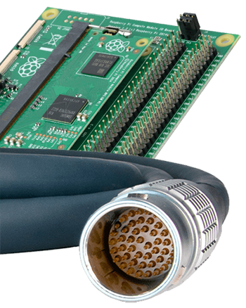
Printed Circuit Boards (PCBs) are across many industrial and consumer electronics, used in products ranging from remote controls to military weaponry. The versatility of PCBs comes from their lightweight, compact, and flexible construction, which can be adapted to suit circuits of any complexity. Though PCBs are relatively commonplace, their complexity makes it critical to source new circuit boards from reliable suppliers. Printed Circuit Board Assembly (PCBA) services harness these complexities.
PGF Technology Group offers comprehensive Printed Circuit Board Assembly services that help our customers fully realize their designs. We have extensive experience working with customers in a broad range of highly innovative industries, including Aerospace, Automotive, Industrial, Medical, and more.
Although the equipment, components, and mounting processes vary significantly between these two assembly methods, we have extensive experience in both techniques. Additionally, we often combine SMT and through-hole technologies for hybrid technology projects.
The silkscreen is a screen-printed layer that provides assembly and reference information for the PCB. The silkscreen is usually white text on the green solder mask.
A solder mask is a protective layer of material applied over the circuit board, serving to insulate and shield conductive traces and prevent solder bridges during the soldering process. The solder mask is responsible for a PCB’s characteristic green color.
Copper layers refer to thin sheets of copper that are laminated onto the surface of the circuit board, forming conductive pathways for electrical signals and power distribution. Every PCB contains one or more copper layers, including the etched pathways (traces) that form the circuit.
Substrate refers to the base material, typically made of fiberglass-reinforced epoxy resin (FR-4), onto which the circuitry and components are mounted and interconnected. It serves to insulate electrical traces from one another.

The most straightforward and most affordable PCBs consist of one copper layer laminated to a non-conductive substrate layer. One side of the board contains all pathways.

A more versatile option, double-sided PCBs incorporate circuitry on both sides of the PCB. These boards have three total layers, consisting of two layers of copper on either side of a non-conductive substrate.

The most complex and expensive, multi-layer PCBs enable intricate circuitry that would be impossible to contain in one or two layers. These boards allow for maximum component density by moving some traces to the board’s interior, freeing room for additional SMT components on the exterior.
Using state-of-the-art machinery, PGF Technology Group can handle surface mount, through-hole, and mixed-technology applications. We also offer integrated electromechanical assembly services for customers seeking larger sub-assemblies or complete products. Electromechanical assembly, or a box build assembly, combines the completed PCB with corresponding electronic components and harnesses to yield a functional product.
Utilizing PGF Technology Group for one-stop, end-to-end assembly of PCBs will ultimately improve the overall quality of the circuit boards, shorten time-to-market, and reduce overall production costs. Our advanced capabilities adhere to the highest industry standards available. From receiving to assembly to testing to shipping, our facility is prepared to process projects with attention and dedication.


Automated assembly is ideal for components that are difficult to solder by hand and high-volume production runs. It is the fastest and most efficient means of producing consistent circuit boards.

Reflow soldering is the most common method used for efficiently soldering SMT-mounted components. The process uses a reflow oven to melt solder onto a pre-heated and pre-soaked PCB.

Wave soldering is another efficient method that involves applying flux to an entire PCB surface, heating the board, and then applying molten solder to the whole heated board. This process has been greatly dismissed due to the addition of selective soldering.

Selective solder is a more precise variation of wave soldering used to apply flux locally rather than the entire PCB. Instead of using a “wave” of molten solder, it uses nozzles to apply solder exactly where needed.

Hand insertion and soldering may be used when project constraints require manual through-mounting.

In-circuit testing (ICT) involves the use of a specialized test fixture that contains probes or pins. ICT verifies the integrity of individual components, checks for proper circuit connectivity, and detects potential defects such as short circuits, open circuits, or incorrect component values.

This automated inspection process uses cameras to scan the PCB for defects and quality issues.

The SPI process closely inspects solder paste deposition before part placement.
PCBAs find extensive applications across various industries, including consumer electronics, automotive, telecommunications, medical devices, industrial equipment, and aerospace. They are utilized in products such as smartphones, automotive control systems, communication devices, medical monitors, manufacturing machinery, and satellite systems, enabling efficient electronic functionality in diverse sectors.

I often rely on the PGF team to provide technical knowledge for working through issues and challenges to optimizing our design for robustness, reliability, and ease of use for the use of our product in manufacturing and end-use application.
Read PGF’s original downloadable eBooks on various electronic manufacturing topics!
Browse our blog post collection to find PCB-related articles about design, assembly, end-use, and more!